1) It is possible for a transistor to act as a closed switch by defining requisite magnitude of saturation level with an equivalent amount of ______.
a. Positive control voltage
b. Negative control voltage
c. Both positive & negative control voltages
d. None of the above
|
Answer
Explanation
|
ANSWER: Positive control voltage
Explanation:
No explanation is available for this question!
|
|
2) Which device plays a significant role in connection of ac source without affecting or causing any sort of perturbation to dc biasing while applying AC to DC biased transistor?
a. Inductor
b. Resistor
c. Coupling Capacitor
d. Filter
|
Answer
Explanation
|
ANSWER: Coupling Capacitor
Explanation:
No explanation is available for this question!
|
|
3) Which biasing method acquires better stability of dc operating point against the variations in β with an assistance of emitter resistor eventually leading to degeneration?
a. Base bias with emitter feedback
b. Base bias with collector feedback
c. Emitter bias with two supplies
d. Fixed current bias
|
Answer
Explanation
|
ANSWER: Base bias with emitter feedback
Explanation:
No explanation is available for this question!
|
|
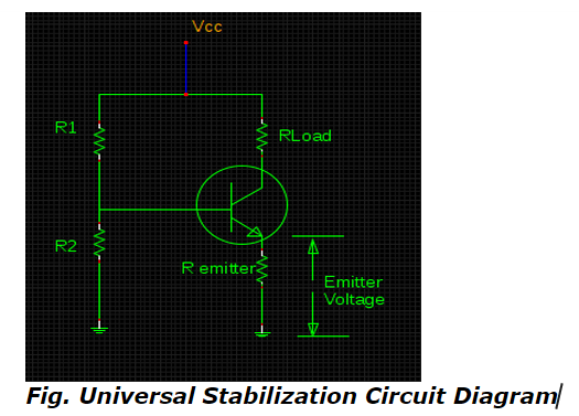
4) What should be the combined value of resistance according to Beta rule especially when the value of βRE is greater than R2 in the following schematic configuration of Universal Stabilization Circuit?
 a.
a. R 2 ¦ βR E
b. R 2 ¦ βR L
c. R 1R 2 ¦ βR E
d. R 1R 2 ¦ βR L
|
Answer
Explanation
|
ANSWER: R2 ¦ βRE
Explanation:
No explanation is available for this question!
|
|
5) The greater level of signal distortion that can be managed by transistor can be visualized in the input static characteristics of common base configuration due to variation in input resistance with respect to ________.
a. Base to emitter voltage
b. Base to collector voltage
c. Base to base voltage
d. None of the above
|
Answer
Explanation
|
ANSWER: Base to emitter voltage
Explanation:
No explanation is available for this question!
|
|
6) Why is the collector region of transistor made larger as compared to emitter region from the physical spacing point of view by reducing the probabilty of transistor inverting?
a. For maintenance of requisite amount of doping level
b. For maintenance of similar polarity with respect to base
c. For maximum power dissipation
d. For maximum allowance of current flow
|
Answer
Explanation
|
ANSWER: For maximum power dissipation
Explanation:
No explanation is available for this question!
|
|
7) What is the major functioning role of VVR in the multistage AGC amplifier circuit during an increment in the signal level?
a. Variation in control of input signal level
b. Variation in voltage gain of multistage amplifier
c. Variation in current gain of multistage amplifier
d. Variation in control of output signal level
|
Answer
Explanation
|
ANSWER: Variation in voltage gain of multistage amplifier
Explanation:
No explanation is available for this question!
|
|
8) The rectified & filtered signal taken at a high level point in AGC amplifier generates _______.
a. dc voltage proportional to the level of an output signal
b. dc voltage proportional to the level of an input signal
c. ac voltage proportional to the level of output signal
d. ac voltage proportional to the level of an input signal
|
Answer
Explanation
|
ANSWER: dc voltage proportional to the level of an output signal
Explanation:
No explanation is available for this question!
|
|
9) How does the FET operate before the pinch-off region with small value of drain-to-source voltage in accordance to the control of drain-to-source resistance by the bias voltage?
a. As a Voltage Controlled Resistor
b. As a Voltage Dependent Resistor
c. As a Voltage-Variable Resistor
d. All of the above
|
Answer
Explanation
|
ANSWER: All of the above
Explanation:
No explanation is available for this question!
|
|
10) How are the zener diodes placed internally in MOSFETs so as to provide defence from the hazardous consequences of stray voltages?
a. Alternately
b. Opposite to each other
c. Back-to-back
d. All of the above
|
Answer
Explanation
|
ANSWER: Back-to-back
Explanation:
No explanation is available for this question!
|
|


